How to judge BGA by X-Ray?
Ailant SMT Test Series:
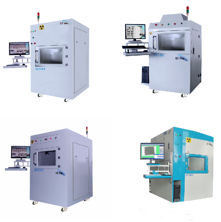
Standard BGA:
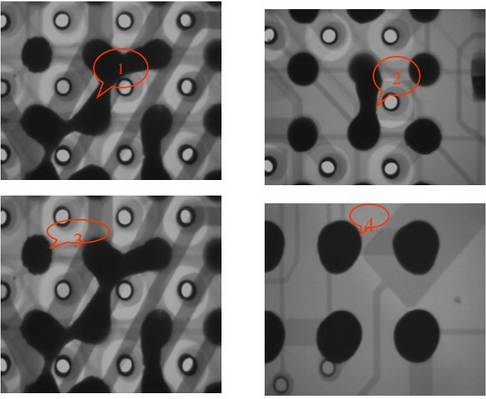
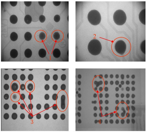
1, image 1, 2 at the joint tin, the reason analysis: there is a problem in the printing solder paste, need to detect the printing link;
2, image 3, there is a jagged shape around the solder ball, the reason analysis: the tin is not enough or the furnace temperature reflow time is short,
Most of this will appear as a phenomenon of soldering;
3, image 4, the solder paste is not uniform, the reflow time is too short, and most of this is a phenomenon of soldering.
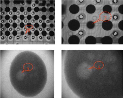
1, the figure 1, 2 Shaoxi, most of the printing links are less printed, it may be the ball;
2, Figure 3, 4 voids, voids The current IPC standard is that the void area cannot exceed 25% of the tin sphere. There are many reasons for the formation of voids.
In particular, the current lead-free process basically has voids, and the root cause of void formation is the melting point of most solder pastes in solder paste.
Too high to be volatilized in time to form a residue. Too large a void area can affect the reliability of the solder joint.
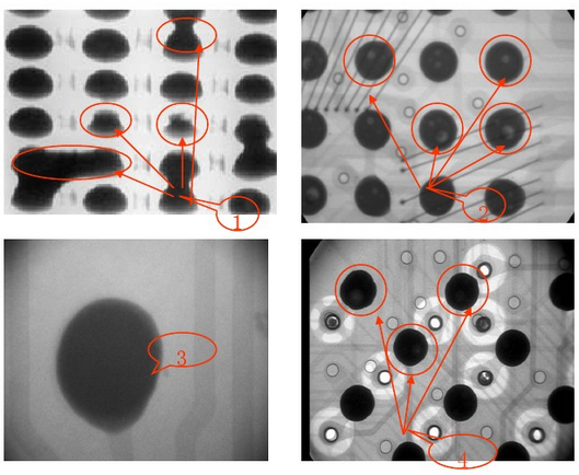
1, Figure 1 oblique image, this board has multiple defects: even tin, less ball, less tin, etc., this board should be a rework board;
2, there are many holes and drifts in Figure 2;
3, Figure 3, 4 solder is not completely molten, that is, cold welding. Most of these are lead-free processes, which should have a higher lead-free melting point and poor wettability.
It is more difficult to control the reflow time or temperature in the reflow furnace.
1, Figure 1 less tin ball, Figure 2 Shaoxi may be a virtual weld. Most of this phenomenon is a problem when printing;
2, Figure 3, 4 is Flip chip, the figure appears multiple failures, less balls, even tin, multiple tin, hollow. The image should be the board after the repair.
Figure 4 shows multiple times of tin, for the same reason as Figure 3.
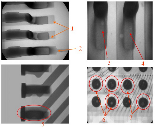
1, Figure 1 is whitish compared to Figure 2, significantly less tin, may not print unevenly;
2, Figure 3, 4 pins are a bit biased, may be misaligned when mounting;
3, Figure 5 bit PLCC shows open circuit, no pin;
4, there are holes in many places in Figure 6, Figure 7 shows a phenomenon of drift, there may be no solder oil here.

National Service Hotline
ELT Technology Co., Ltd. All rights reserved
Address: 3rd Floor, Building B, Building 3, Building 2, Guangshen Road, Chaogang Town, Songgang Town, Bao'an District, Shenzhen, China.
Tel: 0755-29411968
Fax: 0755-27330185
E-mail :elt@elt-usa.com
Website: Http://www.bingjunet.cn

Wechat Public Number

Mobile website